High-performance Fluoropolymers for Semiconductor Processing Equipment
Semiconductors
he plastic materials used in semiconductor fabs have to meet stringent requirements for purity, flammability and chemical resistance. Fluoropolymer materials excel in these areas and these plastics are frequently specified for semiconductor IC chip manufacturing applications. The purpose of this article is to provide an overview of the fluoropolymers used in semiconductor processing and also describe some of the common applications for fluoropolymers in the semiconductor industry.
Semiconductor equipment designers have a wide range of fluoropolymers to choose from including PTFE, FEP, PFA, PVDF, ETFE and ECTFE. These plastics can be divided into two categories: fully fluorinated fluoropolymers (PTFE, FEP and PFA) and partially fluorinated fluoropolymers (PVDF, ETFE and ECTFE). As shown in the graph below, fully fluorinated polymers have lower flexural modulus (stiffness) than partially fluorinated polymers, which means that PTFE, FEP and PFA are softer and easier to bend than PVDF, ETFE and ECTFE. Because of this, fully fluorinated polymers are often used for applications such as flexible tubing where the ability to be bent into position for assembly is required.

Fully fluorinated polymers have higher continuous service temperatures and they typically have broader chemical resistance than partially fluorinated polymers. The graph at the top right shows the higher service temperatures of PFA, FEP and PTFE compared with ETFE, PVDF and ECTFE.


It is important to note that because of their rheology (flow characteristics), PFA, FEP, ETFE, PVDF and ECTFE can be processed using conventional screw extrusion and injection molding equipment. These plastics can also be joined via thermoplastic welding, which allows them to be easily assembled into chemical tanks and wet benches. PTFE has challenging welding characteristics and it must be processed via either ram extrusion, paste extrusion or pressing followed by sintering. This has implications for selecting fluoropolymer stock shapes for semiconductor applications since the plastic chosen must 1) be available in the desired shape and 2) be able to be fabricated as needed to create the final part geometry.
The cost per unit volume of different fluoropolymers varies considerably, as shown in the graph below, with PTFE being the least expensive and ETFE being the most expensive.
Selecting among fluoropolymers generally involves balancing price with mechanical properties, thermal properties, chemical compatibility and processability.
Fluoropolymer composites such as carbon fiber-reinforced PFA have a number of advantages over unfilled fluoropolymers including higher strength and stiffness, better creep resistance and superior dimensional stability. Some fluoropolymer composites are formulated to dissipate static electricity, which helps to prevent IC chip damage from unintentional electrostatic discharge (ESD). Carbon fiber-reinforced PFA materials are often specified for semiconductor applications such as wafer clamps, handling fixtures and end-effectors where chemical resistance, ESD performance, mechanical strength and dimensional stability are required. The photograph to the right shows wafer clamps (black color) manufactured from carbon fiber-reinforced PFA sheet.

Wafer clamps, Shutterstock.
Semiconductor wet processing systems store, transport and apply the chemicals that etch and clean silicon wafers during IC chip manufacturing. Semiconductor fabrication involves a variety of chemistries including high purity water, acids, bases, oxidizers and solvents. Some of these chemicals are used in concentrated forms and process temperatures may be as high as 85°C.
Semiconductor processing chemicals have to meet exacting standards for purity since even trace amounts of contamination can negatively impact IC chip functionality and reduce manufacturing yields. Silicon wafers need to be carefully handled during wet processing operations without being scratched or otherwise damaged from contacting surfaces. Because of these requirements, the plastics used for semiconductor wet process equipment need to meet several design criteria, including:
- Resistance to degradation from the process chemicals
- Resistance to permeation of the process chemicals
- Purity, with only minimal potential to leach, outgas or shed contaminants
- Resistance to the formation of biofilms on their surfaces
- Soft surfaces that won’t damage silicon wafers
- Mechanical and thermal properties suitable for the application
Additionally, certain wet processing applications require plastic materials that comply with FM 4910 and/or NFPA 318 flammability standards. Fluoropolymers tend to outperform other thermoplastic materials for applications where these characteristics are required.
Figure 1 illustrates the outstanding resistance of fluoropolymers to hydrofluoric acid, which is used in the production of semiconductor wafers. As shown on the graph, other plastic materials such as PEEK and polypropylene that are known for their broad chemical resistance become degraded by concentrated hydrofluoric acid at elevated process temperatures.
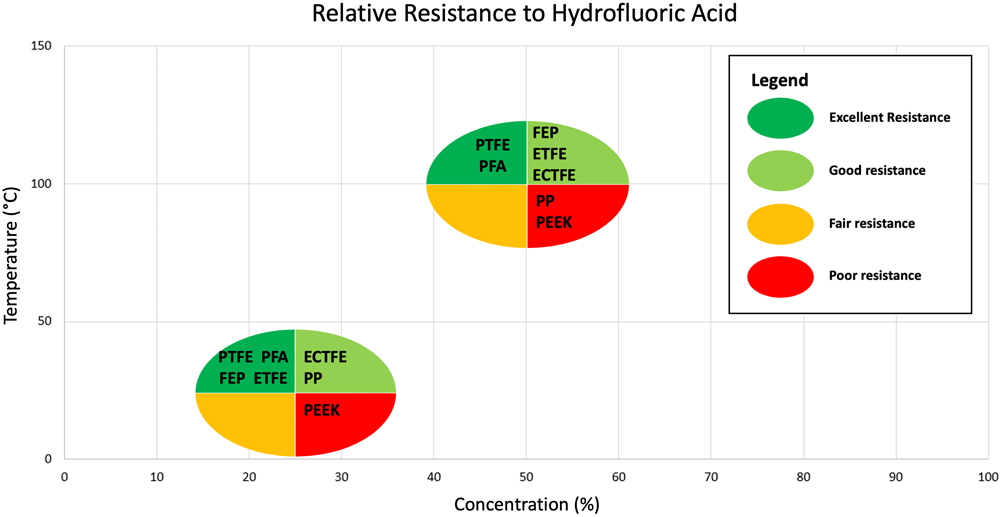
Figure 1
Purity
The semiconductor industry uses fluoropolymers for a wide range of applications. Some of the more common applications that customer-facing employees of IAPD member companies are likely to encounter are discussed below.

PFA tubing use in a wafer processing machine, Shutterstock.
Flexible tubing – PTFE and PFA are often used for flexible tubing in semiconductor processing equipment. The best fluoropolymer for a particular flexible tubing application depends on the required chemical resistance, bend radius, purity, permeability and operating temperature. For example, PFA tubing was used for the chemical delivery system for the wafer processing machine shown in the photograph below.
Wet benches – Components for semiconductor wet benches are frequently manufactured from fluoropolymer materials. The nozzle shown in the photograph above was made from PTFE. The sink was fabricated from PVDF sheet, which was assembled via thermoplastic welding.
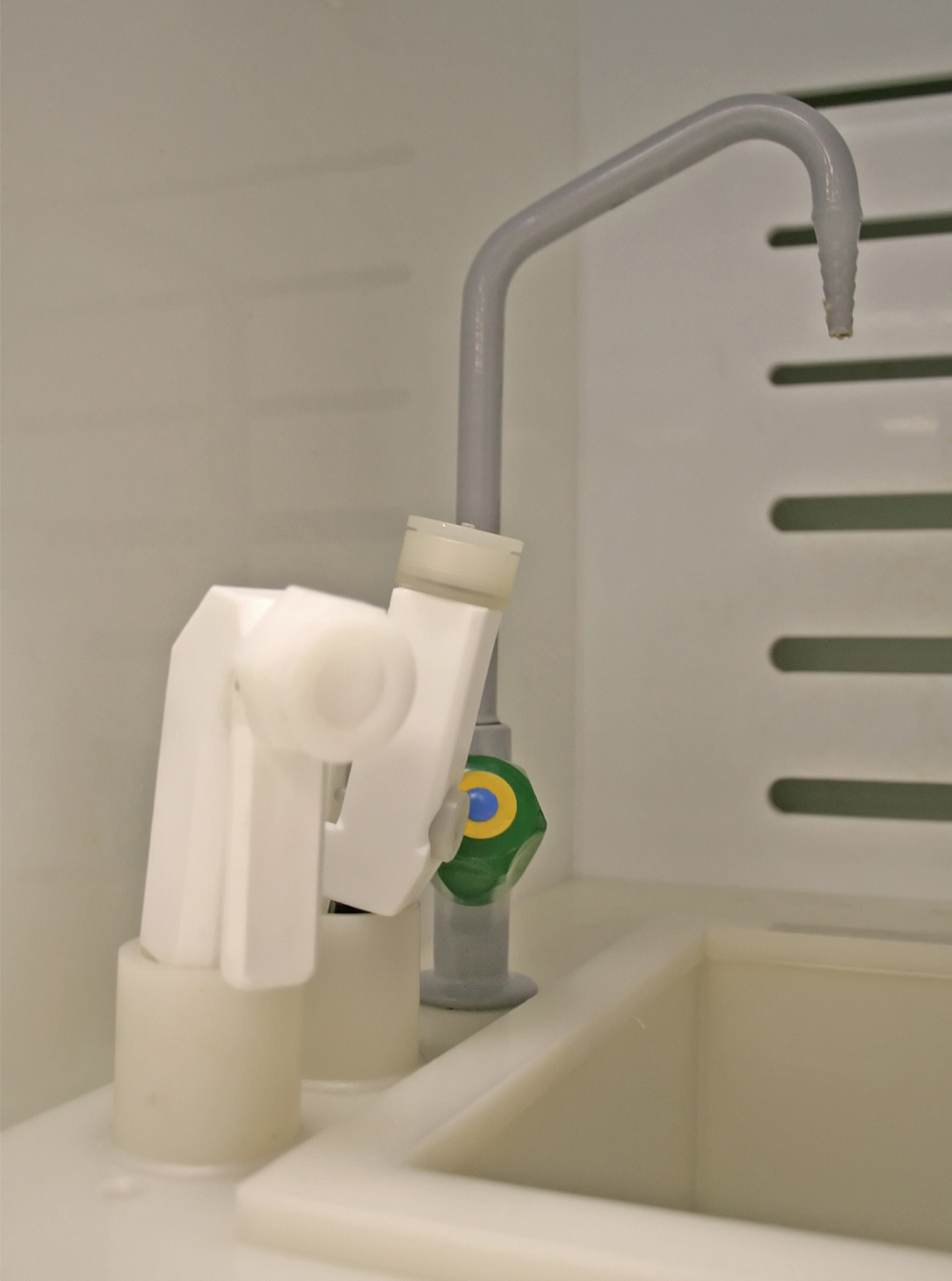
Wet bench with PTFE nozzle and PVDF sink, Shutterstock.

White horizontal wafer supports machined from PTFE with vertical supports machined from PVDF sheet, Shutterstock.
Wafer handling – Fluoropolymers are often used in wafer handling applications since these materials minimize the potential for contamination from leaching, outgassing and shedding, and they can contact wafers without physically damaging them. The white horizontal wafer supports shown in the photograph at the top right were machined from PTFE sheet. PTFE has soft surfaces that won’t scratch IC chips and the purity required to minimize contamination. The off-white vertical supports were machined from PVDF sheet. PVDF has the strength and stiffness required to support the weight of the loaded wafer storage unit.
Other semiconductor applications for fluoropolymers – Additional applications for fluoropolymers in semiconductor plants include chemical tanks, chemical mechanical planarization (CMP) slurry delivery systems, electrical insulators, filters, gas exhaust ducting, pumps, sensors, thermal insulators and the wetted surfaces of valves.
The semiconductor industry is highly competitive and wafer fabs aggressively pursue cost-cutting measures to enhance their profitability. This can lead semiconductor processing equipment designers to consider materials that are less expensive than fluoropolymers for their designs. Additionally, there is increasing pressure from government regulators and environmental groups to limit the use of PFAS materials such as fluoropolymers in industrial machinery.
It is important that performance plastics professionals highlight the value of fluoropolymers for semiconductor IC chip manufacturing so that machinery designers can make informed decisions when selecting plastics for wafer processing applications. Although fluoropolymers are relatively expensive and they require care during manufacturing so that they are produced responsibly, they provide tremendous value to semiconductor companies through cost savings and quality improvements. The benefits of fluoropolymers for semiconductor manufacturing include:
- Improved IC chip yields, with fewer devices failing during final testing. This will become increasingly important as integrated circuit pathways become smaller and more susceptible to damage from even minute amounts of contamination.
- Safer processing of hazardous chemicals compared with other plastics and metals that may more easily fail when exposed to concentrated acids, bases, oxidizers and solvents.
- Reduced risk of fire due to the outstanding flammability characteristics of fluoropolymers compared with other plastic materials.
The purpose of this article has been to provide an overview of the benefits and uses of fluoropolymer materials for the semiconductor industry. As the United States continues to build domestic semiconductor manufacturing capacity, this market is likely to become an increasingly important source of sales revenue for IAPD member companies. Readers interested in learning more about the fluoropolymers used in semiconductor manufacturing are encouraged to read the technical literature published by IAPD member companies who manufacture fluoropolymer stock shapes as well as the articles listed in the references.
- Extrand, C. W. (2003). The use of fluoropolymers to protect semiconductor materials. Journal of Fluorine Chemistry, 122(1), 121-124.
- Hall, L. H. (1996). A materials approach to silicon wafer level contamination issues from the wet clean process, dissertation, December 1996, University of North Texas.
- SAI Semiconductor PFAS Consortium Articles Working Group (2023). PFAS-containing articles used in semiconductor manufacturing. Semiconductor Industry Association.