The Materials Behind the Wafer:
Engineering for Performance and regulatory alignment
semiconductors
by Will Slade, Ensinger
While most plastics make excellent insulators, some wafer handling and test fixture applications seek the advantages of electrically static dissipative (ESD) plastics that bleed off stray or accumulated voltages that would otherwise collect, potentially damaging sensitive conductors on the wafer or chip. The selection and use of these performance plastics are further complicated by a web of international regulatory requirements governing material safety, environmental impact and trade. This article explores critical aspects of this challenging landscape.
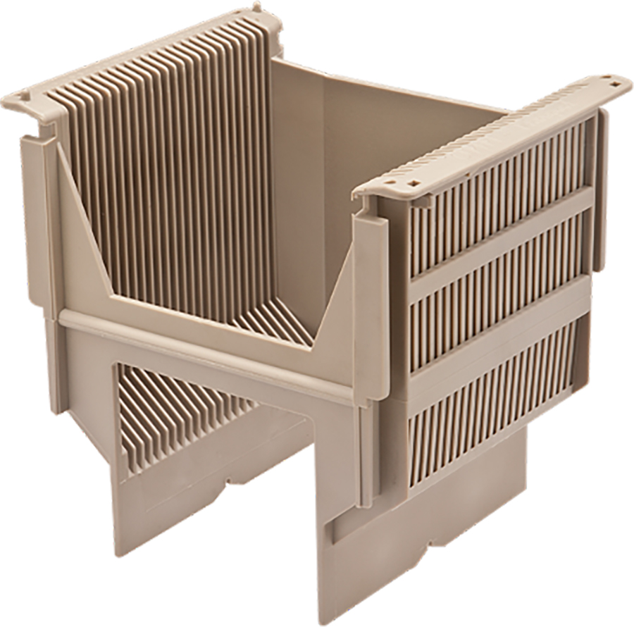
The fixture and test socket materials must be dimensionally stable to maintain the precise alignment of the spring-loaded probes that use the plastic as a combination guide, holder and fixture to contact a chip, chiplet or circuit board. Any thermal deformation could lead to misaligned probes, causing inaccurate test results or even damaging the delicate circuitry.
The challenge of thermal stability is not just about temperature resistance but also about thermal expansion. A low coefficient of thermal expansion (CTE) is vital to ensure that the fixture’s dimensions remain consistent throughout the thermal cycling of the test. When key dimensions are measured in microns, uncontained thermal expansion will compromise test accuracy.
Machinability in this context refers to a material’s ability to be cut, drilled and shaped with high precision, minimal tool wear and a clean finish. The intricate geometries of semiconductor test fixtures, which can feature complex cavities, channels and fine-pitch holes, demand a material that can be machined with exceptional accuracy.
High-performance plastics like PEEK, polyetherimide, PEI, PAI and Polyimide are excellent candidates for Computer Numerical Control (CNC) machining in the semiconductor industry. These materials offer specific properties that are advantageous for precise manufacturing:
- Low stress levels: Materials with low internal stress minimize the risk of warping during and after machining, which is crucial for maintaining tight tolerances.
- Minimal burr formation: The formation of burrs (small, raised edges of material) during machining can compromise dimensional accuracy and potentially contaminate the cleanroom environment. Using the right material, along with optimized machining parameters, helps to minimize burr formation.
- Dimensional stability: The ability of the plastic to maintain its shape and size under mechanical stress is essential for creating reliable fixtures.
The choice of machining technique also plays a role. CNC machining has become the standard for producing complex plastic components for semiconductors due to unmatched precision and repeatability. But the human element still matters — hats off to the many talented toolmakers who understand these materials, as managing the speeds, feeds and dimensional characteristics is art as well as science.
- Restriction of Hazardous Substances (RoHS): This EU directive restricts the use of specific hazardous materials in electrical and electronic equipment. For semiconductor plastics, this means avoiding materials containing heavy metals like lead, mercury and cadmium. Compliance requires manufacturers to reformulate materials and implement rigorous testing to ensure parts are safe.
- Registration, Evaluation, Authorization and Restriction of Chemicals (REACH): Another EU regulation, REACH, mandates the registration of chemicals and restricts the use of certain hazardous substances. This has significantly increased documentation requirements and production costs for semiconductor components, including plastics, by requiring transparency in chemical compositions.
- Per- and Polyfluoroalkyl Substances (PFAS): Emerging regulations, particularly in the EU and some U.S. states, are targeting PFAS — often called “forever chemicals” — due to their persistence in the environment. This could pose a major challenge for the semiconductor industry, which relies on high-performance fluoropolymers (such as PTFE and FEP) that contain PFAS.
International Organization for Standardization (ISO) standards, such as ISO 9001 for quality management and ISO 14001 for environmental management, are critical for demonstrating compliance and ensuring consistent manufacturing processes. For plastic components specifically, ISO standards define requirements for characteristics like measurement tolerances, crucial to high-precision components.
Formed in 1898, ASTM International (formerly the American Society for Testing and Materials) is a not-for-profit global leader in the development and delivery of voluntary consensus standards. ASTM standards provide standardized methods for testing and evaluating the physical, mechanical and chemical properties of plastic materials, covering a wide range of tests from tensile and impact strength to chemical resistance and environmental exposure. ASTM standards for semiconductor plastics focus on critical properties like low outgassing (ASTM E595), chemical resistance (ASTM D543) and electrical insulation (ASTM standards for electrical insulating materials).
SEMI has been used to create more than 1,000 industry approved Standards and Safety Guidelines in key topics including safety, materials, packaging, traceability and cybersecurity in order to improve semiconductor manufacturing operations and several SEMI standards apply to testing plastics for their suitability in key process areas.
The role of plastic components in semiconductor manufacturing is understated but crucial. Their thermal and mechanical stability and machinability are core facilitators of wafer and electrical testing, while regulatory compliance ensures their safe, ethical and environmentally sound use. As the industry continues its relentless drive toward miniaturization and higher performance, the demand for innovative plastics that can meet increasingly stringent requirements will only grow. Success in this evolving landscape will hinge on a deep understanding of material properties, manufacturing processes and the complex web of regulations that govern the semiconductor ecosystem.