Thermoplastic Material Selection in a Semiconductor Manufacturing Plant
semiconductors
by Dr. Tim Biggs, Roechling Industrial Gastonia
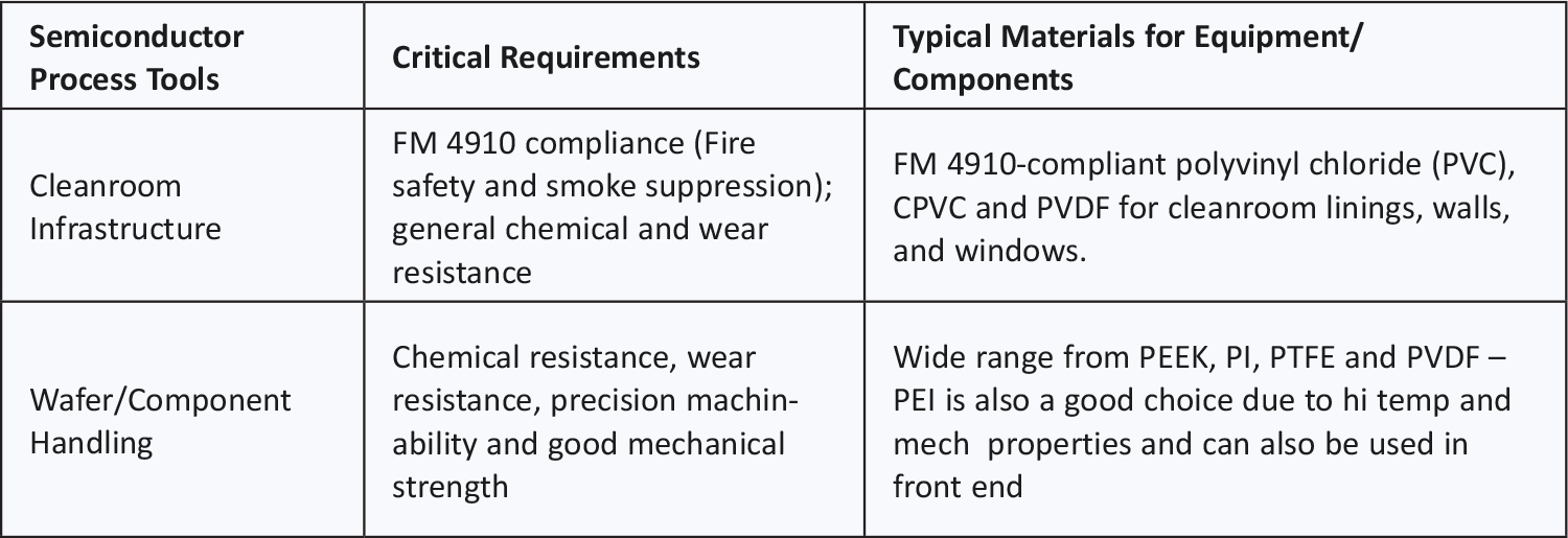
aterial selection is a critical and complex challenge in semiconductor manufacturing, driven by the need for ultra-high purity, extreme precision, and resistance to harsh processing environments. While the primary chip material is typically silicon (or other III-V materials like Gallium Arsenide), specialized high-performance plastics are essential for the manufacturing equipment and cleanroom infrastructure.
The technical selection criteria for these support materials are stringent, focusing on factors like:
- Contamination Risk: Ultra-low outgassing and leachables to prevent micro-contamination of the wafer.
- Chemical Resistance: Impermeability to corrosive acids, solvents, and plasma used in wet and dry etching.
- Thermal and Dimensional Stability: Ability to maintain shape and performance under high-temperature processes and precision machining requirements.
- Electrostatic Dissipation (ESD): Proper electrical properties for materials used in wafer handling and fixturing.
- FM 4910 Compliance: Flame retardant materials for cleanroom construction.
Material selection also requires examination of commercial factors like pricing, availability and supply chain considerations. However, this article will describe technical material selection across the key semiconductor manufacturing stages, referencing the insights provided by Roechling on specialized plastic applications in the semiconductor industry.

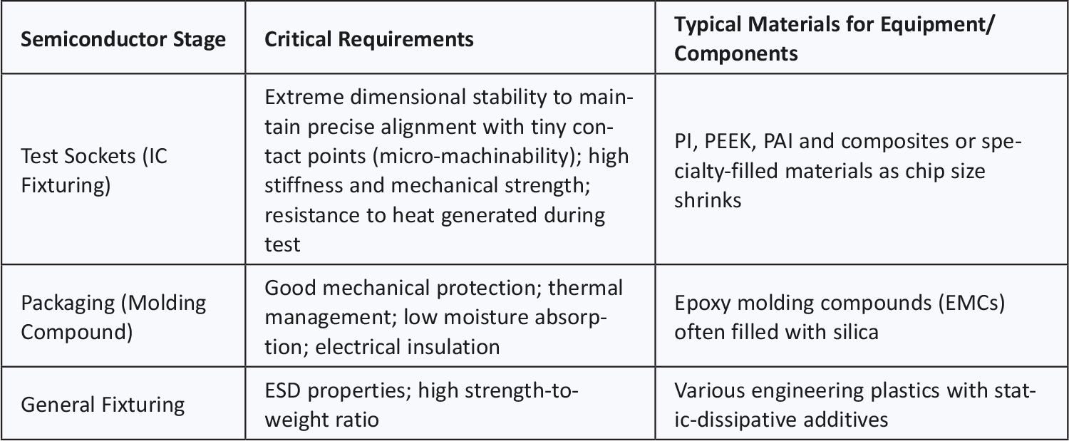
The selection of materials in semiconductor manufacturing is a dynamic process where trade-offs between chemical resistance, purity, dimensional stability and temperature performance are constantly evaluated. As feature sizes continue to shrink (approaching the sub-nanometer node), the demand for increasingly specialized and high-purity engineering plastics like PEEK, PTFE, PVDF and PI for process tools and test equipment becomes even more critical to ensure the integrity of the integrated circuits.
Dr. Tim Briggs is the Semiconductor Business Development Manager at Roechling Industrial Gastonia. For more information, contact Roechling Industrial Gastonia at 903 Gastonia Technology Parkway, Dallas, NC 28034-7791, USA; by phone at (704) 922-7814; or online at www.roechling.com/us/industrial